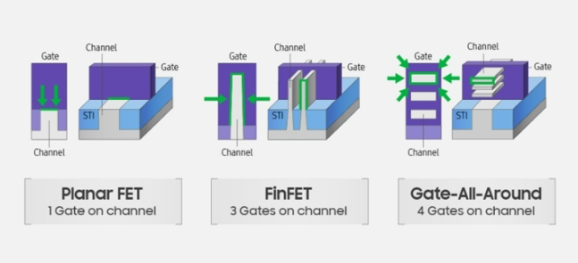
Samsung Electronics’ unique “GAA” (Gate-All-around) technology is considered a winning move that can catch up with Taiwan’s TSMC at once. We looked at GAA technology that will change the game in foundry (semiconductor consignment production) industry.According to industries on the 26th, Samsung Electronics is planning to officially announce mass production of 3-nano semiconductor processes based on next-generation GAA technology this week. Samsung Electronics unveiled its plan to start mass-production of 3-nano products in the first half of this year, which is earlier than TSMC, at the foundry forum in October last yearChoi Si-young, president of Samsung Electronics’ foundry division, expressed confidence in preoccupying next-generation transistor technology by saying that it plans to mass-produce first-generation 3-nano semiconductors in the first half of 2022 and second-generation 3-nano semiconductors in 2023.
Industries predict that if Samsung Electronics starts mass-production of 3-nano as scheduled, it will secure technology leadership in next-generation semiconductor processes and become a stepping stone to lead TSMC. Unlike Samsung Electronics, TSMC is currently called FinFET for developing and mass-producing 3-nano products be in the same processTransistors, which are the basic elements of semiconductor chips, are semiconductor devices that make digital information composed of binary methods of ‘0’ and ‘1’ into electrical signals. The transistor controls the signal by allowing the gate to act as a ‘switch’ and to flow and disconnect current to the channel.
To place as many semiconductor chips as possible on a silicon wafer of a limited area, the size of the transistor must be as small as possible. In addition, power consumption should be minimized to reduce heat generation and increase battery life. The history of semiconductor power generation is a process that has made transistors smaller and faster, while simultaneously consuming less powerPinpet, which was applied by Samsung Electronics from the 14-nano process in 2012, is a three-dimensional structure in which silicon channels established in the form of gates and bumps mesh on three sides. The thin and long-established channel resembles the back fin of a fish, so it was named “Fin” transistor. Currently, most semiconductors are mass-produced by this pinpet process.
Designed to overcome the limitations of the pinpet process, it is the GAA process in which the gate wraps the channel in all directions. Furthermore, Samsung Electronics has improved its wire-shaped channel structure into a thin paper-shaped “nanosheet” called “MBCFET™” The process was built independently.
It is predicted that 3-nano process that uses MBCFET™ structure, which is Samsung Electronics’ own GAA technology, will improve performance by 30% compared to 5-nano process based on Finpet, and will reduce power consumption by 50% and area by 35%. Although specific figures may vary during the actual mass production process, it is clear that power efficiency and performance improve overallIt is heard that Samsung Electronics has also secured customers through 3-nano process.

In the foundry industry, the preemptive introduction of the latest process, which is faster than competitors, is used as a marketing point, and securing a small number of high-tech process customers is considered the key to generating profitabilityWhen U.S. President Joe Biden visited Samsung Electronics’ Pyeongtaek Campus last month, the scene where he signed a 3-nano prototype instead of a general guest book led to Samsung Electronics’ technology being known worldwide. It left a strong impression on customers by showing that technology is ahead of competitors in state-of-the-art processes.

Since 2019, Samsung Electronics has been making efforts to secure customers by distributing the initial version of 3-nano GAA’s ‘Process Design Kit (PDK)’ to major fabless (semiconductor design company). Its strategy is to secure products that fit its foundry process as future customers by designing them in advance and accelerating their release.
Again, the key is to secure a stable yield (the ratio of accepted products without defects). Samsung Electronics suffered from speculation that it would give up or postpone production of 3-nano process even before mass-production of 2-nano process two years ago due to yield problems. There were also concerns that major customers left due to delayed improvement in yield of 4-nano semiconductors.
“Samsung Electronics’ announcement of mass production of 3-nano means that it has secured minimum yield, but considering the difficulty of the process, it will take some time to raise the yield to sufficient level,” an industry source said.
EJ SONG
ASIA JOURNAL


